Intel recently held its 2025 Direct Connect event in San Jose, California, primarily to showcase the latest advancements in its foundry business. At this conference, Intel routinely presented its process technology roadmap, with a particular emphasis on the 14A process, the successor to 18A, and 18A derivative processes. New CEO Pat Gelsinger also underscored the future direction of Intel Foundry at the event, highlighting breakthroughs in process technology, the expansion of advanced packaging solutions, and close collaboration with industry partners.
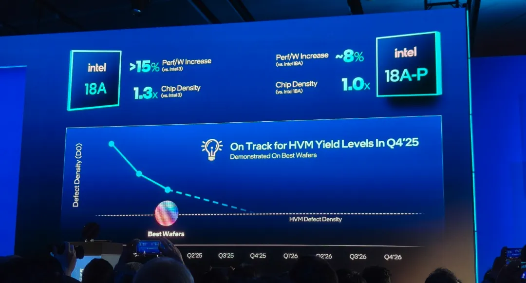
The Intel 14A process was one of the central highlights of the conference. This process has entered the early testing phase and is slated for mass production in the second half of 2026. 14A utilizes the second-generation backside power delivery technology, PowerDirect (an upgrade from PowerVia), which optimizes energy efficiency and performance by directly providing power contacts to transistors. Compared to traditional frontside power delivery designs, PowerDirect moves power lines to the backside of the wafer, reducing signal interference and improving transistor density and circuit efficiency. Intel stated that 14A will be among the first to adopt ASML’s high numerical aperture extreme ultraviolet lithography (High-NA EUV) equipment, further shrinking feature sizes and enhancing chip performance. Intel has already deployed two High-NA EUV machines at its D1X factory in Oregon and plans to use both high and low NA lithography in 14A production to balance cost and precision. Furthermore, 14A will continue to employ Intel’s second-generation RibbonFET gate-all-around (GAA) transistor architecture. Compared to traditional FinFET designs, this architecture allows for more precise current control, reduces leakage, and increases transistor density. Intel claims that 14A will offer a 15-20% improvement in performance-per-watt, a 25-35% reduction in power consumption, and approximately a 1.3x increase in transistor density. These technological advantages position Intel about two generations ahead of TSMC in backside power delivery technology, laying a technical foundation for its competition in the high-end chip market.
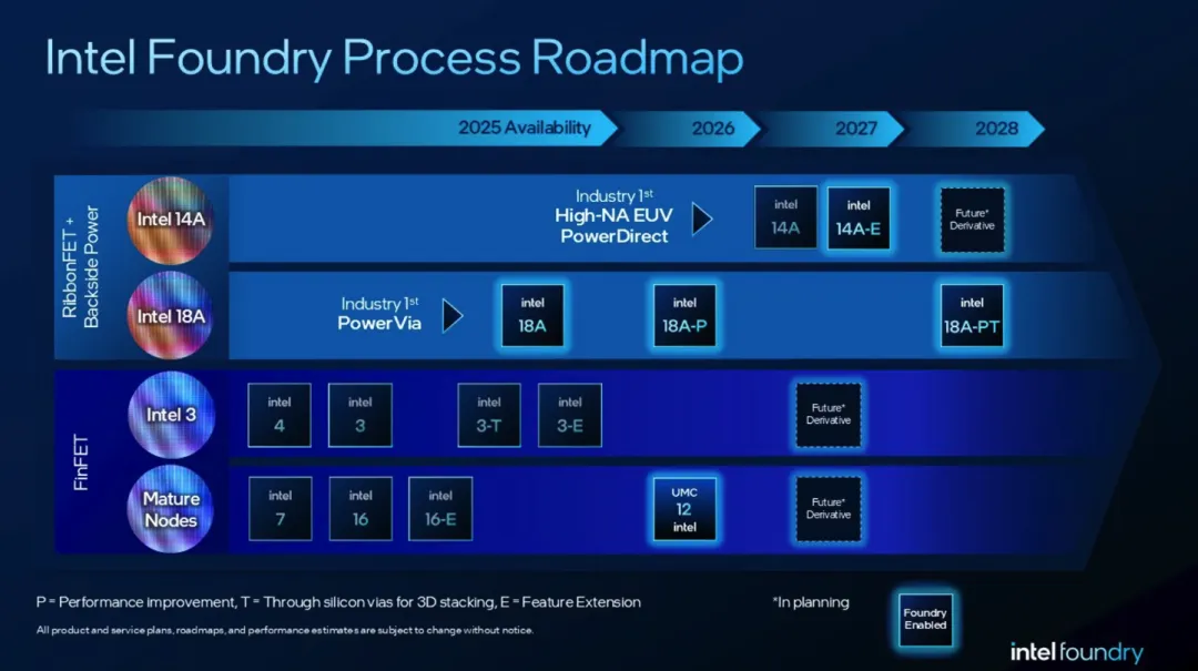
Concurrently, Intel further expanded its 18A process family with the introduction of two derivative processes: 18A-P and 18A-PT. 18A-P is a performance-oriented process offering higher performance gains compared to the original 18A node, making it suitable for high-performance computing and client devices. 18A-PT introduces Foveros Direct 3D hybrid bonding technology, supporting interconnect pitches of less than 5 microns, which is superior to TSMC’s SoIC-X with a 9-micron pitch. This high-density, low-resistance 3D stacking technology enables Intel to develop processor architectures similar to AMD’s Ryzen X3D, enhancing performance and bandwidth efficiency through vertical stacking of multiple chips. 18A-PT will be used in the next-generation Clearwater Forest Xeon server processors, providing higher computing density and energy efficiency for data centers. Intel revealed that the 18A process has entered the risk production phase and is scheduled for high-volume manufacturing (HVM) by the end of 2025. The first products to utilize 18A include the Panther Lake AI PC client processor and the Clearwater Forest server processor, with mass production planned for early 2026. Intel also stated that version 1.0 of the 18A process design kit (PDK) has been released to customers, and external clients will complete their first chip tape-outs in the first half of 2025.
Intel’s advanced packaging technology was also a key focus of the conference. Intel continues to innovate in the 2.5D and 3D packaging domains, introducing various solutions to meet the needs of both client and data center applications. EMIB (Embedded Multi-die Interconnect Bridge) 2.5D technology enables low-cost, high-efficiency connection between logic chips and high-bandwidth memory (HBM) via a silicon bridge and has been in mass production since 2017. The upgraded EMIB-T incorporates through-silicon vias (TSVs), supporting more flexible IP integration. The Foveros family encompasses a range of 2.5D and 3D packaging solutions, with Foveros-S 2.5D optimized for client applications using a 4x reticle silicon interposer, in mass production since 2019. Foveros-R and Foveros-B 2.5D are expected to enter production in 2027, utilizing redistribution layers (RDL) and silicon bridges, respectively, to meet complex heterogeneous integration requirements. Foveros Direct 3D employs copper-to-copper hybrid bonding interfaces, offering ultra-high bandwidth and low-power interconnects suitable for high-performance computing scenarios. Additionally, Intel introduced EMIB 3.5D packaging, combining EMIB and Foveros technologies to integrate multiple 3D stacks within a single package. A representative application is Intel’s Data Center GPU Max series SoC, which features over 100 billion transistors, 47 active tiles, and 5 process nodes, making it Intel’s most complex heterogeneous chip to date.
The development of Intel Foundry’s ecosystem has also made progress. Intel is deepening its collaboration with EDA (Electronic Design Automation) and IP vendors such as Synopsys, Cadence, Siemens, and Ansys to ensure seamless integration of its process nodes with industry standards. These partners have validated tools and design flows for 18A and 14A, supporting customers in accelerating chip design. Furthermore, Intel has partnered with Arm to launch the “Emerging Businesses Initiative,” providing foundry services for Arm-based system-on-chips (SoCs), including IP support, manufacturing capabilities, and financial assistance, to help startups innovate. Intel has also attracted several ASIC customers, including Microsoft, NVIDIA, Broadcom, and Faraday, to adopt the 18A process, with Microsoft planning to use 18A for its in-house designed chips. Early sampling results of 18A chips have been well-received by customers, who consider their performance and reliability to exceed expectations.
Intel’s 18A process directly rivals TSMC’s N2 (2nm) process. Intel holds an advantage in energy efficiency and area efficiency due to its PowerVia backside power delivery technology and RibbonFET GAA transistors. In contrast, TSMC’s N2 is expected to enter mass production in 2025, while backside power delivery technology will not be introduced until the N2P process in 2026. Intel anticipates that 18A will surpass N2 in performance-per-watt and production cost, potentially winning more foundry orders. The introduction of the 14A process further solidifies Intel’s long-term competitiveness, and by 2027, Intel will achieve broader application coverage through 14A-E (an enhanced version).
Meanwhile, Intel is exploring immersion liquid cooling technology, aiming to support the heat dissipation needs of 2000W TDP chips by 2030. Additionally, Intel plans to introduce glass substrate technology in 2027 to further enhance packaging performance and signal integrity.
Intel Foundry’s goal is to become the world’s second-largest foundry by 2030, with a current expected deal value exceeding $15 billion. With breakthroughs in the 14A and 18A processes, a diverse range of advanced packaging technologies, and a maturing ecosystem, Intel is accelerating its efforts to catch up with TSMC and Samsung. The Direct Connect 2025 event showcased Intel’s technological prowess, offering technology enthusiasts a glimpse into the next generation of chip manufacturing technology. However, the ultimate outcome remains to be seen.